Projectsプロジェクト
Photonic Materials and Devices Group
Prof. Takashi KITA and Assistant Prof. Yukihiro HARADA
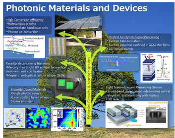
Molecular-beam epitaxial growth of semiconductor nanostructures
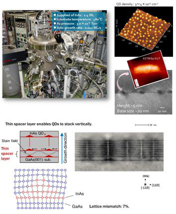
When the size of the semiconductor becomes smaller on the order of the de Broglie wavelength (several tens of nanometers or less) of electrons and electron holes, tDevelopment of ultra-violet (UV) light emitting devices he degree of freedom of motion of electrons and holes becomes restricted, and it is possible to achieve high efficiency radiation and high non-linearity at specific wavelengths. In our laboratory, we are working towards achieving an expression of a completely new functionality by employing Molecular Beam Epitaxy (MBE) technology to create two-dimensional quantum wells, one-dimensional quantum wires, and zero-dimensional quantum dots. In particular, quantum dots have the characteristic feature of being able to form "naturally" by means of self-assembly, and this is a very futuristic approach that harnesses the power of nature. When the compound semiconductor InAs is fed onto a GaAs substrate or InP substrate, InAs quantum dots several nanometers in size are formed by self-assembly at a high density (several hundred per square micrometer), depending on the balance between the lattice constant and surface energy. In our laboratory, we use various techniques like Scanning Probe Microscopy (SPM), Transmission Electron Microscopy (TEM) and Photoluminescence Spectroscopy, to demonstrate the self-assembly process of the quantum dots and the expression of optical properties never seen before. We are currently researching next-generation device materials including polarization independent semiconductor optical amplifiers (SOA), broadband light sources and solar cells that will enable high energy conversion efficiency, using quantum dots with such high-controllability.
Route for high conversion efficiency solar cells
The solar energy that reaches the earth is about 1kW per square meter. With the solar energy that reaches the earth in one hour, it is possible to provide the energy consumed by the entire world for one year. In other words, we would be able to create the power required by the entire world if we installed solar cells on just one percent of the total area of the earth. If we had to replace the current power supply infrastructure with solar cells, we would need to lower the power generation cost to 7 JPY/kWh, comparable to power for use by business. It is said that a 40% energy conversion efficiency of solar cells is needed for this purpose. In order to achieve this objective, we need to make use of a new concept, a new high-tech material, and establish both ultra-high efficiency and low cost. It is expected that the concentrating solar cells that make use of quantum structure would allow for the realization of this objective. Concentrating solar cells concentrate the incidence of solar light using a lens, and the semiconductor cells used for injecting the solar light onto a solar cell are small in size. This can achieve both ultra-high conversion efficiency and low cost. The energy conversion efficiency of a solar cell is determined primarily by the loss caused by the transmission without any absorption by the semiconductor and the loss caused by the surplus light energy that becomes the heat inside the semiconductor. In our laboratory, we are conducting research and development of a new type of solar cell that greatly suppresses these losses by making use of quantum dots, quantum wells and superlattices. In particular, the theoretical value of the conversion efficiency in intermediate band solar cells is expected to exceed 60% during the maximum concentration of light.
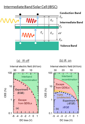
Development of intermediate-band solar cells
Quantum-dot superlattice intermediate-band solar cell
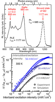
Intermediate band solar cells (IBSCs) have attracted considerable attention because, under maximum concentration, an extremely high conversion efficiency exceeding 60 % can be expected. An IB placed in the bandgap enables additional absorption, valence band (VB)-to-IB and IB-to-conduction band (CB), in addition to the ordinary interband absorption from the VB to the CB. However, the conversion efficiency of IBSCs has not yet exceeded that of single junction SCs, because of several issues. In particular, the weak intersubband absorption (IB-to-CB) limits the efficiency. It is necessary to increase the intersubband absorption strength to a level equivalent to the interband absorption by reducing the carrier recombination rate. Generally, as the IB is provided by the quantized states of nanostructures, the electron–hole recombination rate for the photoexcited carriers in the confined system tends to increase, causing the reduced electron density in the IB to weaken the intersubband absorption coefficient. It has been reported that the conversion efficiency drastically decreases as the electron lifetime decreases. So far, an extremely long electron lifetime of 1 ms in the IB has been reported in the IBSC utilizing InAs QDs confined in a GaAs/AlGaAs quantum well at room temperature. Such a long electron lifetime is accomplished by separating the excited electrons from the holes thermally escaping from the quantum well at room temperature. In contrast, when the electrons and holes are excited in the QDSL minibands, the carriers in the miniband can be spatially separated in the internal electric field, and an improved intersubband absorption of the IB-to-CB increases the two-step photocurrent.
- Y. Okada et al., J. Appl. Phys. 109, 024301 (2011).
- T. Kada et al., Phys. Rev. B 91, 201303 (Rapid Communication) (2015).
- Y. Okada et al., Appl. Phys. Rev. 2, 021302 (2015).
- Y. Harada et al., Phys. Rev. B 93, 115303 (2016).
- T. Tanibuchi et al., Phys. Rev. B 94, 195313 (2016).
- S. Watanabe et al., Appl. Phys. Lett. 110, 193104 (2017). APL Editor's Picks
- T. Kada et al., Scientific Reports 7, 5865 (2017).
- K. Hirao et al., Appl. Phys. Express 11, 012301 (2017).
Dot-in-well (DWELL) intermediate-band solar cell
We studied in detail the photocurrent generation process in two-step photon absorption in intermediateband solar cells including InAs quantum dots embedded in AlGaAs/GaAs quantum wells at room temperature. The photocurrent generated by the two-step photon absorption exhibited saturation as the interband excitation intensity increased in strength. On the other hand, as the intersubband excitation intensity increased, the two-step photo-excitation current deviated from a power law. Furthermore, the two-step photo-excitation current exhibiting saturation and deviation strongly depended on both the interband and intersubband excitation intensities. To interpret these phenomena, we performed a theoretical simulation of the two-step photo-excitation current. The results suggest that the photocurrent saturation and deviation were caused by filling of the intermediate states with electrons. Furthermore, our calculated results indicate that the electron-recombination lifetime in the intermediate states is extremely long. The results of the temperature dependence of the two-step photo-excitation current and the excitation intensity dependence of photoluminescence suggest that efficient electron-hole separation extends electron lifetime. In order to retrieve the electron lifetime from the decay profile, we developed a model reproducing the observed decay and performed parameter fitting. The fitting results indicate that the electron lifetime in the DWELL is greater than 100 μs. In the two-color excitation time-resolved photocurrent measurement, we found that an additional infrared (IR) light fastens the photocurrent decay while the photocurrent increases by approximately 3%, because the additional IR light causes two-step photoexcitation of electrons in the DWELLs towards the conduction band. Furthermore, we demonstrated that the open-circuit voltage increases with increasing of the contribution of the second IR excitation process.
- S. Asahi et al., J. Appl. Phys. 116, 063510 (2014).
- S. Asahi et al., IEEE Journal of Photovoltaics Vol. 6, No. 2, 465~472 (2016).
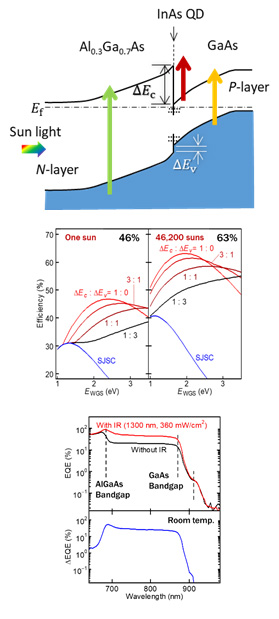
Development of two-step photon up-conversion solar cell (TPU-SC)
Reducing the transmission loss for below-gap photons is a straightforward way to break the limit of the energy conversion efficiency of n-i-p semiconductor solar cells (SCs). We have proposeed a TPU-SC with a hetero-interface comprising different band-gaps of Al0.3Ga0.7As and GaAs. In the TPU-SC, a series of two-step photoexcitation accomplishes the up-conversion. By absorbing a below-gap photon, an electron transits from the valence band to the conduction band of the narrow bandgap material. Upon absorbing another below-gap photon, the electron accumulated at the hetero-interface is further pumped into the conduction band of the wide bandgap material. This ideal TPU process following the absorption of two below-gap photons produces additional photocurrent with boosting the photovoltage depending on the band offset at the hetero-interface. The below-gap photons for Al0.3Ga0.7As directly excite GaAs and generate electrons at the hetero-interface. The densely accumulated electrons at the hetero-interface are pumped upwards into the Al0.3Ga0.7As barrier by below-gap photons for GaAs. Efficient TPU is achieved by introducing InAs quantum dots at the hetero-interface. We observe not only a dramatic increase in the additional photocurrent, which exceeds the reported values by approximately two orders of magnitude, but also an increase in the photovoltage.
- S. Asahi et al., Nature Communications 8, 14962 (2017).
- S. Asahi et al., Scientific Reports 8, 872 (2018).
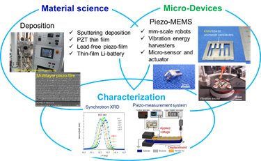
Development of ultra-violet (UV) light emitting devices
Ultra-violet (UV) light is indispensable for various industrial processes such as lithography, curing, polymerization using photochemical reactions, sterilization, and medical treatment. For these applications, many kinds of discharge lamps using mercury have been widely used in such fields. However, mercury is recognized as a chemical of global concern due to its long-range transport in the atmosphere, its persistence in the environment, its ability to bio-accumulate in ecosystems and its significant negative effect on human health and the environment. For human life free from mercury, it is strongly desired to develop novel UV lighting source which can replace currently available mercury lamps. Recently, nitride-semiconductor based UV light emitting diodes (LEDs) are attracting strong interest. In LEDs, the emission wavelength can be controlled by the optical band gap, and efficient light emission is realized by utilizing quantum structures. However, the external quantum efficiency becomes extremely small in the UVB (280-320 nm) and UVC (200-280 nm) wavelength regions. Moreover, the spectral line width limited by the thermal carrier distribution near the band edge causes a relatively broad emission-band width being generally over 10 nm, and the flux from a small LED chip must be controlled to prepare uniform power distribution on the large area when we need to irradiate large area with the UV light. For photo lithography to obtain the high resolution and medical applications to avoid unexpected side effects, light panel with a narrower spectral width is essential. Instead of using band-edge emission, we focus on the use of narrow band emissions from the intra-orbital electron transitions of rare earth ions. Rare earth ions are widely used in various phosphors, solid state laser crystals, and optical amplifiers. In this work, we focus on gadolinium (Gd) which emits a typical narrow-band UVB luminescence near 310 nm. Improving the emission intensity and reducing the fabrication cost offer a practical and sustainable solution to the challenge for launching the device. We developed two kinds of UV light sources of plasma tube arrays (PTAs) and cold cathode fluorescent lamps (CCFLs) with using an oxide phosphor containing Gd3+ ions. PTAs have been widely used for wide display devices, and CCFLs are well known as a bright, low-cost, low-power consumption light source which can be practically used for back light applications. As compared with a spot-type light source such as LEDs, these fluorescent lumps are suitable for fabricating wide light emitting panels at a low cost. Here, we fabricated UVB light panels emitting at ~310 nm, which drives up the output power to 10 mW/cm2. We compare detailed emission properties with characteristics of UV-LEDs and also clarify superiority for medical treatments.
Mesoscopic and Plasmonic Materials Group
Prof. Minoru FUJII
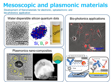
We develop colloidal solutions of all-inorganic silicon-based nanocrystals in the size range from the quantum confinement regime (~10 nm, quantum dots) to the dielectric anntenna one (~200 nm), and explore the application in electronics, optoelectronics, photonics, biophotonics, etc.
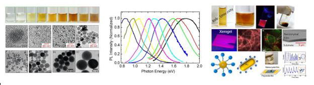
We develop plasmonic nanostructuers and nanocomposites for sensing and upconversion applications.
Bioproduction Engineering Group
Prof. Chiaki OGINO and Associate Prof. Tsutomu TANAKA
Research Interests
- Yeast breeding for bio-refinery
- Ethanol fermentation from cellulosic material
- Metabolic engineering in Streptomyces
- Protein expression by fungi and Streptomyces
- Application of AFM to bimolecular interaction assessment
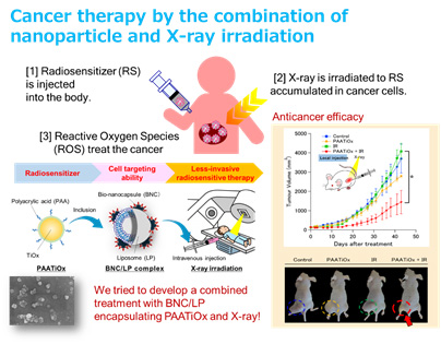
- Application of nanoparticle to cancer therapy
Inorganic Materials Chemistry Group
Prof. Minoru MIZUHATA
The Laboratory of Applied Inorganic Chemistry focuses the properties, behaviors, and reactions of inorganic compounds and its composites through the various experiments using physicochemical and electrochemical technique. We employ many experimental methods in order to make clear these objects on the basis of the viewpoint form "IONS, ELECTRONS, and WATER". Students are encouraged through the experimental works through the preparation of novel materials, development and improvement of the experimental apparatus, and the discussion of the experimental results.
Last decades, we are focusing the materials chemistry for the future technology and industrial chemistry through the R&D on various kinds of nanotailored materials. Structure and properties of electrolyte solution, solution chemistry in the hetero-phase systems, synthesis of metal oxide thin films by the Liquid Phase Deposition Method, and fabrication techniques of polymer-metal nanoparticle composites by the Relaxative Auto Dispersion method have been studied. We have published more than 100 papers for last 10 years and obtained valuable suggestion and encouragements from many scientists and engineers all over the world.
Structure and Properties of Highly Concentrated Aqueous Solution
The structure and properties of highly concentrated aqueous solution depend on the interaction among the dissolved species shuch as water molecules and ionic species. Although the concentrated solution are utilized in the various industrial fields, there is little research on them. We focuses the structure and properties of the solutions using various experimental methods, such as an condictivity measurement, X-ray diffraction and RDF, spectroscopic measurement, etc, to make clear the interaction among the dissolved species.
Properties of Liquid Phase in the Solid/Liquid Coexisting Systems
Highly dispersion systems, such as paste and slurry are important materials for industrial field. In such solid/liquid systems, the properties of liquid phase near the surface of the solid phase varied with a decrease of the liquid content. We studies how the properties of liquid phase changes in the vicinal region on the solid surface. The part of this subject is proceeded under the support by the Proposal-Based New Inductry Creative Type Technology R&D Promotion Program from the New Energy and Industrial Technology Development Organization of Japan (NEDO)
Preparation of Ultra Fine Metal Particles by Relaxative Auto Dispersion (RAD) Method
The novel preparation method for ultra fine metal particles with the crystalization process of amorphous matrix was found in our laboratory. We proceed the resolving the dispersion process and the development of the metal-dispearsed composite materials.
Preparation of Metal Oxide Thin Films by Liquid-Phase Deposition (LPD) Method
The liquid phase deposition using hydrolysis reaction of fluoro-metal complexes has been developped in order to prepare the metal oxide thin films. This technique is "Soft Process" using aqueous solution reaction. We proceed the research on the optimization of the reaction condition and properties of formed thin files.
Material-surface Engineering Group
Associate Prof. Tatsuo Maruyama
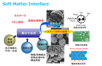
Interfaces and surfaces play important roles in living systems and artificial functional materials. For instance, adsorption of solutes, extraction, wettability, cells and energy production involve interfaces and surfaces to work. Our group tries to develop surfaces (or interfaces) that have novel functional properties based on polymer chemistry, organic chemistry, biochemistry and surface engineering. Some of our research interests are gels, surfactants and polymers that have novel and unique characteristics derived from self-assembly or cooperation of molecules and micromaterials.
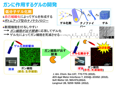
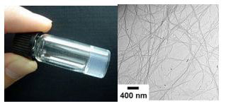
Supramolecular gelator (low-molecular-weight gelator)
Although gels are usulally prepared using polymers (gelatin, agarose), gels can be prepared by low-molecular-weight gelators (supramolecular gelators). Low-molecular-weight gelators (supramolecular gelators) spontaneously self-assemble to form nanofibers or nanosheets and to behave like polymers, leading to gelation of solvents. We developed various types of supramolecular gelators and succeeded in the gelation of water, organic solvents and ionic liquids at low concentrations. Our goals are to develop funtional gels using supramolecular gelators, which are higly-conductive ionogels, hydrogels exhibiting anti-cancer activity and gels available for chemical reactions.
We recently synthesized
- Supramolecular gelator that can harden a wide variety of water, organic solvents and ionic liquids.
- Supramolecular gelator that can kill cancer cells.
- Supramolecular gelators that can harden ionic liquids (conductive ionogel).
- These gels have potential to be used in pharmaceutical and medical fields and also in electronic device.
- Y. Nishida el al., Angew. Chem. Int. Ed. accepted (2017).
- W. K. Restu el al., Colloid Polym. Sci.295, 1109-1116 (2017).
- Y. Eguchi et al., Chem. Commun., 53, 5802-5805 (2017).
- T. Kataoka et al. ACS Appl Mater Interfaces 7, 23346–23352 (2015).
- A. Tanaka et al., J. Am. Chem. Soc. 137, 770-775 (2015).
- Y. Ishioka et al., Soft Matter 10, 965-971 (2014).
- N. Minakuchi et al., Langmuir 28, 9259−9266 (2012).
- D. Koda et al., Chem. Commun., 46, 979-981 (2010).
Surface functionalization of polymer using polymer segregation.
Material sufaces plays particularly important roles in our lives and industry. Touching, wetting, hitting, confining etc involve material surfaces in all aspects of physical phenomena. We try to develop the methods to control the physical and chemical properties. Here we design and synthesize functional polymers, and coat material surfaces with the functional polymers to control the surface properties. Our goals are to develop non-fouling surfaces, catalytically active surfaces, surfaces that can recognize target molecules in a specific manner to be utilized for separation technique and chemical analysis.
- Development of ultra-violet (UV) light emitting devices.
- R. Hiraoka et al., Chem. Comm., 51, 17447-17450 (2015).
- S. Shiota et al., Langmuir 31, 8824-8829 (2015).
- S. Yamamoto et al. Langmuir 31, 125-131 (2015).
- A. Shimomura et al. Langmuir, 29, 932-938 (2013).
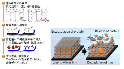
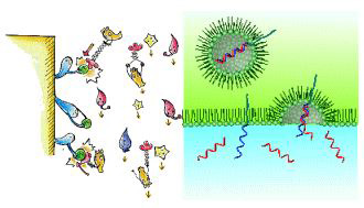
Design and synthesis of functional surfactants that can exceed conventional detergents.
Surfactants are widely used as detergents. We try to develop surfactants that have novel functions beyond "washing detergents". For example, the figure shows the surfactants that have "separation ability". We developed a surfactant having oligo DNA, which can separate complemtary DNA, and a surfactant that can recognize proteins to be introduce on a membrane surface. These surfactants successfully separate and purify target DNA, RNA and proteins that were produced by enzymatic reactions and recombinant E. coli. We would like to expand these achievements to the fundamental techniques required for the future industry and biotechnology.
- T. Maruyama et al., Chem. Commun., 52, 12376-12379 (2016).
- C. Higashi et al., RSC Adv., 6, 88244-88247 (2016).
- T. Maruyama et al, ChemNanoMat, 2, 461-465 (2016).
- T. Kato et al, RSC Adv. 4, 57899-57902 (2014).
- T. Honjo et al., Anal Biochem., 434, 269-274 (2013).
- T. Maruyama et al. RSC Adv., 2, 125–127 (2012).
- T. Maruyama et al., Chem. Commun., 4450-4452 (2007).
Design and formation of microstructures prepared by electrospinning and electrospraying
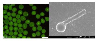
The electrospinning/electrospraying technique has a great potential for preparation of nano- and micro-fibers because of the simplicity of the apparatus, its high productivity and its easy setup. During the past decades, the electrospinnning technique has attracted more and more attention as novel techniques of nanotechnology and microtechnology. We employed the electrospinning/electrospraying technique to prepare polymeric and inorganic microcapsules, and short fibers functionalized with biomolecules. We also succeeded in the living-cell encapsulation in microcapsules using the electrospray technique.
- T. Matsuura et al., Colloid Polym. Sci. 7, 39937(2017).
- T. Matsuura etl al., Colloids Surf. A 526, 64-69 (2017).
- Y. Funasaki et al. Colloid Polym. Sci. 292, 3049-3053 (2014).
- A. Yunoki et al., ACS Appl. Mater. Interfaces 6, 11973–11979 (2014).
- T. Maruyama et al. RSC Adv., 2, 11672–11674 (2012).
- Y. Fukui et al. Colloids Surf. A, 370, 28-34 (2010).
Recycling of precious and rare metal ions using protein-rich biomass.
Recently, the prices of precious metals and rare metals fluctuate violently because of drastic increases of an industrial demand and a speculative factor. These metals may be contained in industrial wastes. Effective use of precious metals and the rare metals can be achieved by separating and collecting them from such a waste solution. There are already several methods for recycling these metals but these methods have some drawbacks to a varying degree. On the other hand, metal ions in vivo form complexes with various biomolecules (proteins and saccharides) and they exhibit unique functions. This lets us speculate that it is possible to selectively separate and collect the metal ions using biomolecules. In this study, we tried to develop the technique for recycling precious metals from industrial wastes by using protein-rich biomass (egg-shell membrane).
- T. Maruyama, et al., Process Biochem. 49, 850-857 (2014).
- T. Maruyama et al., Environ. Sci. Technol. 41, 1359-1364 (2007).
- T. Maruyama, et al., J. Colloid Interf. Sci. 447, 254–257 (2015).