This is a web page of MI-1 lab. in Department of Mechanical Engineering, Kobe University.
|
|
Nano Electro Mechanical
Systems Lab. [MI-1] Isono Lab.@ Department of Mechanical Engineering. Kobe Univ. |
[Japanese Version] |
Message to Kobe University Students
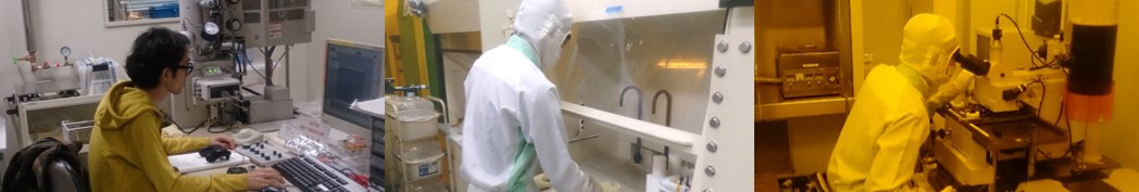
In MI-1 lab, we work on researches on leading-edge academic fields in micro and nano sciences and engineering with micro electro mechanical systems (MEMS) technology.
We have a wide research fields where micro and nano engeneering is nessesary, with a concept of new creation and invention of micro-machining technology for next generations. We research on
invention of nano-scale semiconductor materials, development of new application devices based on micro sensors and actuators, and study on bio-chemical and medical fields.
The laboratory aims to practice world-class leading-edge research. For example, we already have world-class achievements on the the research on physical properties evaluation of new nano semiconductor materials using MEMS technology, and we are working on international joint researches with several European research institutes.
In bio-chemical MEMS researches, we have won various academic awards, and joint researches with companies has been started.
These researches are promoted by cooperation of all lab members, based on "Material mechanics", "Mechanical engineering", and "Fluid engineering" as well as "Phisics" and "Semiconductor engineering".
Our lab has research environment in which you can practice from theoretical design and fabrication of MEMS to measurement and evaluation consistently.
Through these researches, we primally expect to students to laern practical academic skills, problem-solving skills, and logical ideas whch are needed for international-level professional engineers and researchers.
We welcome visiting of students who want to practice the world's leading-edge researches, who are curious and inquisitive, who want to challenge new things, or who want to learn how to solve problems.
Reserch fields

Details:[Research]
(1) Challenges for multiphysics characterization of low-dimensional nano semiconductors
◆Mechanical and electrical evaluations of nano-scale structures using MEMS technology
◆Mechanical and electrical evaluations of carbon-based nanowires
1. FIB-deposited carbon nanotubes (CNT)
2. Multi-walled carbon nanotubes (CNT)
◆Material properties elucidation of silicon-based nanowires under giant elastic strain field
1. Single crystal silicon nanowires' mechanical properties at room temperature
to intermediate temperatures
2. Mechanical and electrical properties of n-type silicon nanowires grown by VLS bottom up process
3. A piezo resistive effect of p-type single-crystal silicon nanowires patterned by top-down processes
4. Giant-strain-induced physical properties of core-shell (C/S) 3C-SiC nanowires
grown by VLS bottom-up processes
(2)Study for new systhesis of low-dimensional nanowire materials
◆ Synthesis of carbon nanotubes (CNT) with a density control
◆ Establishment of growing techniques of silicon nanowires usign a VLS-CVD process
(3) Development of new MEMS application devices
◆ Development of individually-driving multi-probe cantilever array for low-cost
scanning probe parallel nanolithography (SPNL) in the atmosphere
and development of patterning techniques for nanopatterning using it.
◆ Development of length-controllable SPM cantilevers with integrated actuators
for topology evaluation of both solid and soft surfaces
◆ Development of gas-sensing devices using a MEMS resonator with integnated CNT
for trace hydrogen gas detection
◆Development of MEMS-based tiny tactile sensors for minimally invasive medical treatments
(4)Fabrication of plasmonic nanostructures and application to bio/chemical sensors with a high sensitivity
We research on fabrication techniques of plasmonic nanostructsres, based on techniques of gold nano particle synthesis and nano particle arrangements. As applications of the techniques, we also research on a technique for single-molecular detection using surface-enhanced raman spectroscopy (SERS) and on bio/ chemical sensing with a high sensitivity.◆ Micro fluidic devices for gold nano particle synthesis by a high-speed liquid mixing
◆ Arrangement techniques of nano particles
◆ Bio-chemical analysis techniques using SERS with arranged gold nanoparticles
◆ Micro and nano fluidic devices for SERS with linearly-arranged gold nanoparticles
◆ MEMS-resonator devices for laser's frequency detection using optical-thermal conversion on
periodic gold nanostructures
※ We also work on joint researches with domestic and foreign research institutes for rsearches related to maicromachines and nanomachines.