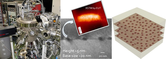
半導体のサイズが電子・正孔のド・ブロイ波長程度(数10 ナノメートル以下)まで小さくなると電子・正孔の運動の自由度が制限されるため、特定の波長で高効率に発光させたり、高い非線形性を実現することができます。私たちの研究室では分子線エピタキシー(MBE)技術を駆使して、2次元の量子井戸、1次元の量子細線、0次元の量子ドットを作製し、これまでにない全く新しい機能の発現を目指しています。特に量子ドットは自己形成によって“自然”に形成できることが特徴で、自然の力を利用した大変未来的なアプローチです。化合物半導体のInAsをGaAs基板やInP基板上に供給すると、格子定数と表面エネルギーのバランスによって、数nmサイズのInAs量子ドットが高密度に(1 mm角あたり数百個)自己形成します。研究室では走査プローブ顕微鏡(SPM)、透過型電子顕微鏡(TEM)、フォトルミネッセンス分光法などさまざまな手法を駆使して、量子ドットの自己形成プロセスとこれまでにない新しい光物性の発現を明らかにしています。このような高い制御性をもつ量子ドット利用して、偏波に依存しない半導体光アンプ(SOA)をはじめ、広帯域光源、高いエネルギー変換効率を可能にする太陽電池などの次世代で実現が期待されているデバイス材料を研究しています。
Nano-epitaxy of Semiconductors(Kita)When the size of the semiconductor becomes smaller on the order of the de Broglie wavelength (several tens of nanometers or less) of electrons and electron holes, the degree of freedom of motion of electrons and holes becomes restricted, and it is possible to achieve high efficiency radiation and high non-linearity at specific wavelengths. In our laboratory, we are working towards achieving an expression of a completely new functionality by employing Molecular Beam Epitaxy (MBE) technology to create two-dimensional quantum wells, one-dimensional quantum wires, and zero-dimensional quantum dots. In particular, quantum dots have the characteristic feature of being able to form "naturally" by means of self-assembly, and this is a very futuristic approach that harnesses the power of nature. When the compound semiconductor InAs is fed onto a GaAs substrate or InP substrate, InAs quantum dots several nanometers in size are formed by self-assembly at a high density (several hundred per square micrometer), depending on the balance between the lattice constant and surface energy. In our laboratory, we use various techniques like Scanning Probe Microscopy (SPM), Transmission Electron Microscopy (TEM) and Photoluminescence Spectroscopy, to demonstrate the self-assembly process of the quantum dots and the expression of optical properties never seen before. We are currently researching next-generation device materials including polarization independent semiconductor optical amplifiers (SOA), broadband light sources and solar cells that will enable high energy conversion efficiency, using quantum dots with such high-controllability.
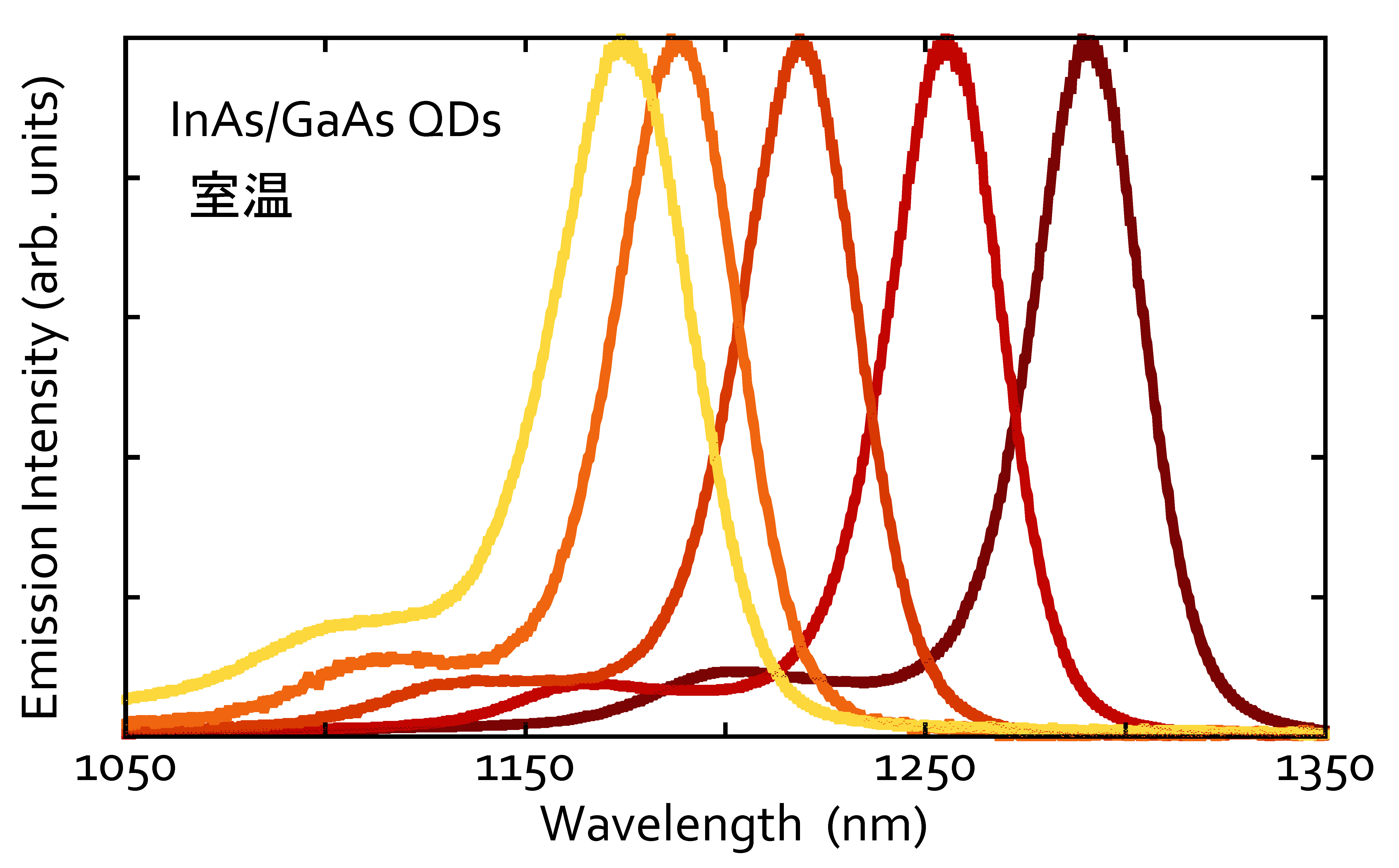
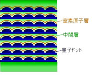
このような高機能光デバイスに利用される量子ドットは、サイズや密度など求められる条件がデバイスごとに異なるため、”自然”に形成される量子ドットの構造を要求に応じて制御することが不可欠です。本研究室では、多様な量子ドット構造の作製を目指して、MBEによる結晶成長のメカニズムや作製手法について研究を進めています。具体的には窒素原子層を導入した量子ドットの積層成長が挙げられます。中間層を介して量子ドットを3次元的に配列させた構造(量子ドット超格子)はデバイスの高機能化を実現する鍵となる構造ですが、従来の手法では基板材料と量子ドット材料との格子定数の違い(格子歪)による結晶欠陥の発生や、量子ドットのサイズ、形状の変化が問題となり、30層を超える量子ドットの多層化は困難です。本研究では、格子歪の影響を軽減する効果が期待される窒素原子層を導入して、30層以上の量子ドットの積層構造の実現を目指します。
Creation of a variety of quantum dot structures (Kita)Required conditions such as size and density of quantum dots that are used in the highly functional optical devices differ for every device. So it is essential to control the structure of quantum dots that are formed “naturally” by self-assembly to suit these requirements. In this laboratory, we are working towards the creation of a variety of quantum dot structures and are studying the mechanism of MBE crystal growth due to MBE and manufacturing methods. To be specific, we are researching the stacked growth of the quantum dots in which a nitrogen layer is introduced. A structure made of a three dimensional array of quantum dots (a quantum dot superlattice), through an intermediate layer is the key to achieving device high performance. However, with conventional techniques, the occurrence of crystal defects and changes in the size and form of quantum dots caused by the difference in the lattice constants (lattice strain) of the substrate material and the quantum dot material has posed a problem and it has become difficult to produce a multi-layered structure of quantum dots with more than 30 layers. In this study, we strive to achieve a quantum dot stacked structure with more than 30 layers by introducing a nitrogen layer, which is expected to reduce the impact of lattice strain.
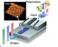
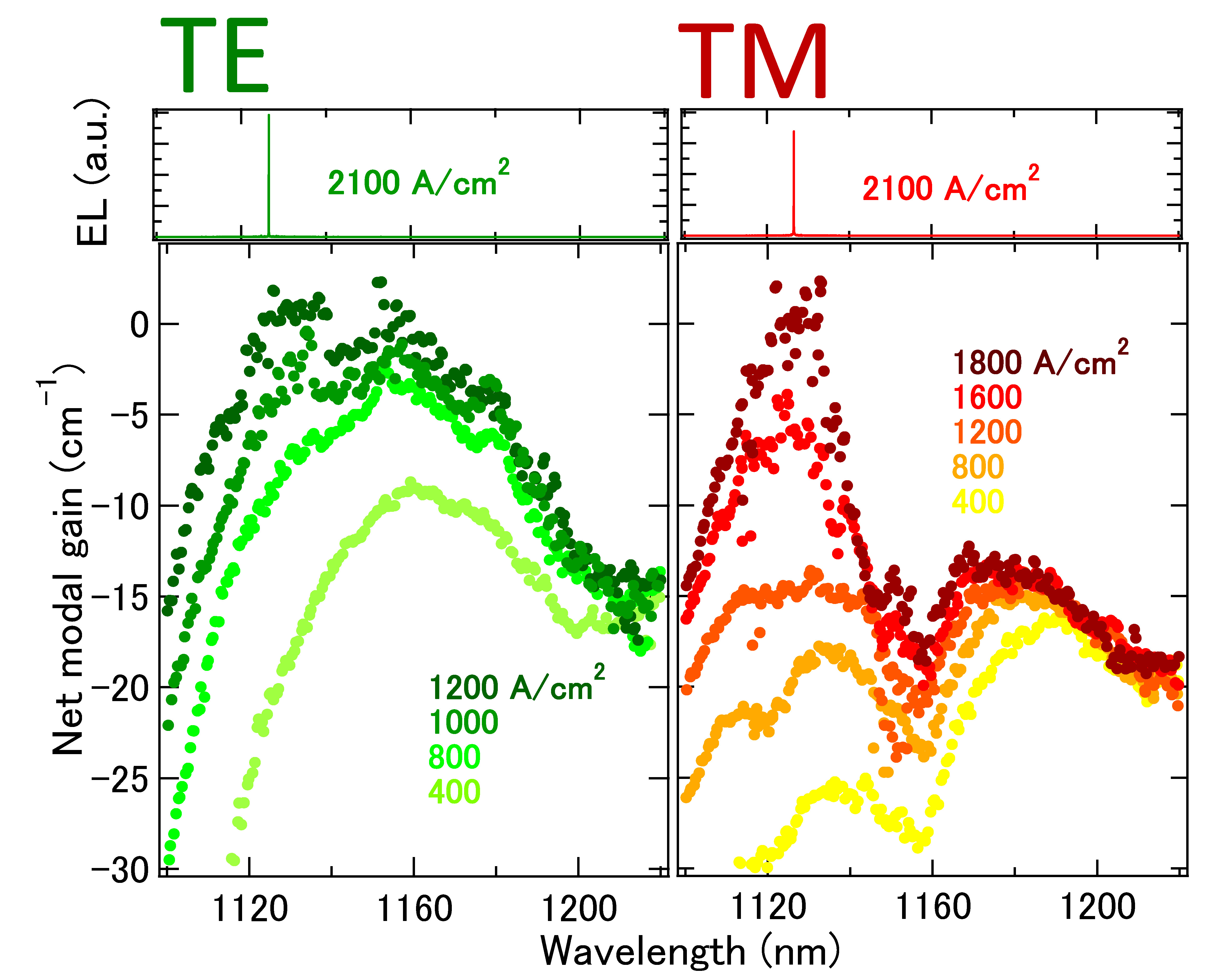
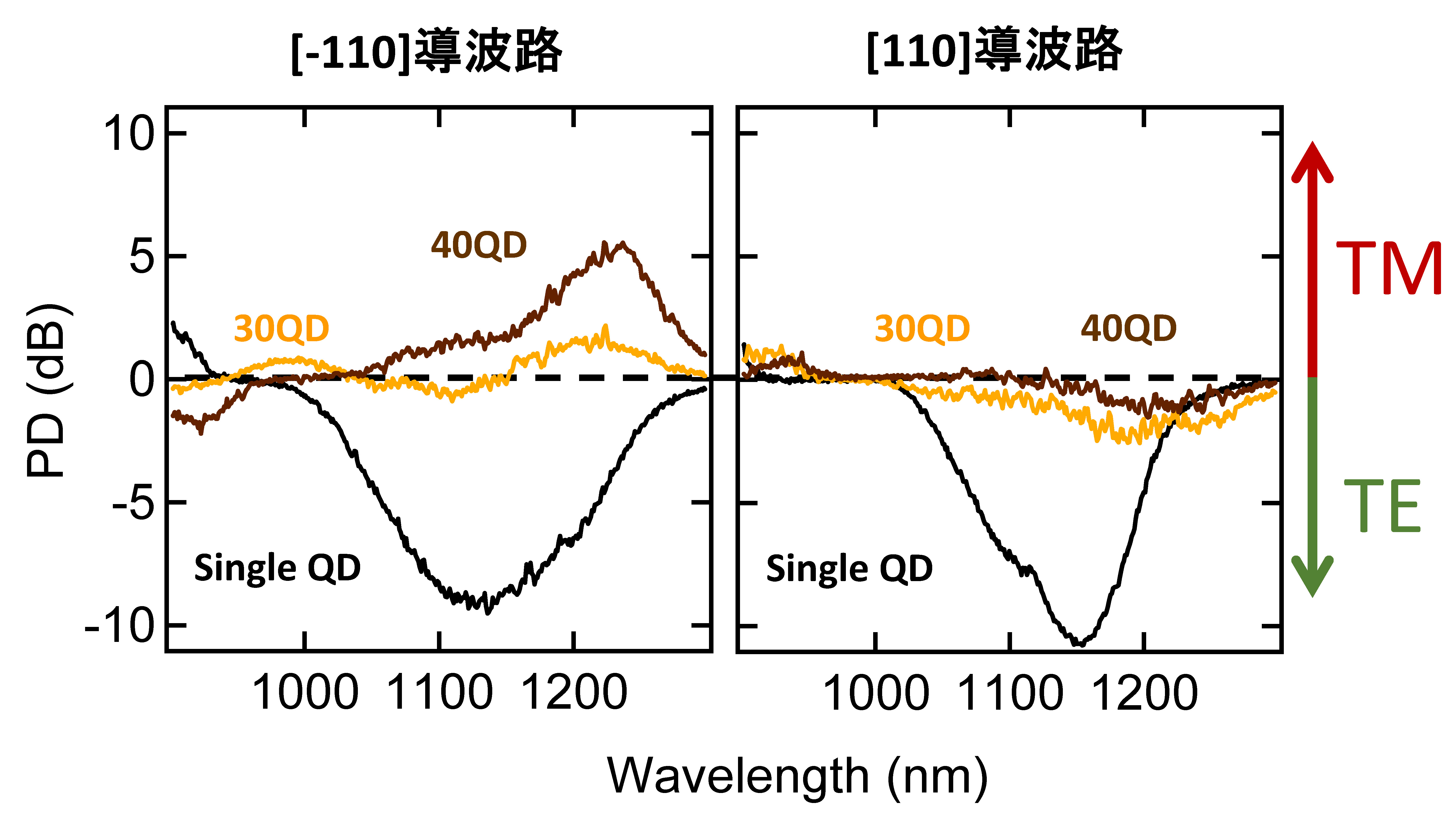
超高速な次世代光ネットワークでは光による信号伝送だけでなく、中継点での光による信号増幅や高速な信号処理が不可欠です。そのような中継デバイスの要となるのが半導体光アンプ(Semiconductor Optical Amplifier:SOA)です。SOAは手のひらサイズで、100 Gb/s以上で動作する超高速光パルスの3R(Reamplification再増幅,Reshaping再整形, Retaiming再同期)光再生中継機能や超高速な光スイッチングを実現します。しかし従来の量子井戸を利用したSOAでは量子井戸に平行な偏光成分の増幅利得が圧倒的に大きく、偏光波面が乱れた光ファイバ伝搬光のSOA出力は入力信号を忠実に再生できません。わたしたちはナノ形状を制御した独自量子ドットを利用して偏波無依存な光応答特性を世界で初めて実現しました。具体的には積層成長したInAs量子ドットを活性層に含む半導体光アンプ構造を作製し、電流注入による発光特性において1.3μmの光通信波長帯で400nm超のスペクトル幅を有する偏波無依存動作を実証しています。
Development of broadband polarization independent semiconductor optical amplifiers (Kita)In addition to signal transmission, signal amplification by light at relay points and high-speed signal processing are also indispensable to ultra-high-speed, next generation optical networks. The Semiconductor Optical Amplifier (SOA) is the keystone in such relay devices. The SOA is a palm-sized device that realizes the 3Rs (namely Reamplification, Reshaping and Resynchronization) of the high-speed optical pulses that move at more than 100 Gb/s, the optical regenerative repeater function and high-speed optical switching. However, in the SOA that use conventional quantum wells, the amplification gain of the polarized light component that is parallel to the quantum well is extremely large, and the amplified signal amplitude of the transmitted light is unexpectedly deformed by such anisotropic amplification. So it is not possible to faithfully reproduce the input signal as the SOA output. We were the first in the world to achieve polarization independent optical response characteristics using unique quantum dots whose nano-sizes are carefully controlled. To be specific, we created a Semiconductor Optical Amplifier structure that included the InAs quantum dot stack in the active layer, and demonstrated polarization independent behavior with a spectral width of more than 400 nm, at an optical communication wavelength band of 1.3 μm under electrical current injection.
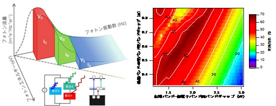
地上に到達する太陽エネルギーは、1平方mあたり約1kW。 地球に届く太陽エネルギー1時間分の量で世界全体が1年間に消費しているエネルギーすべてをまかなえます。別の言い方をすれば、 地球全体のたった1%の面積に太陽電池を設置すれば、世界中が必要とする電力を創り出すことが可能なのです。現在の電力供給インフラを太陽電池で置き換えるには、発電コストを事業用電力なみの7円/kWhまで落とさねばなりません。そのために必要とされる太陽電池のエネルギー変換効率は40%と言われています。この目標を達成するには、新概念、新素材を活用し、超高効率化と低コスト化を両立させる必要があります。これを実現すると期待されているのが、量子構造を利用した集光型太陽電池です。集光型太陽電池は太陽光をレンズで集光して太陽電池に入射するため用いる半導体セルのサイズが小さく、超高変換効率と低コストを両立できます。太陽電池の発電効率は半導体に吸収されずに透過してしまうロスと余剰光エネルギーが半導体内で熱となるロスによって主に決まります。われわれの研究室では、量子ドットや量子井戸(超格子)を駆使してこれらロスを格段に抑制した新しいタイプの太陽電池構造の開発研究を行っています。特に、中間バンド型太陽電池では、変換効率の理論値はなんと最大集光時最高60%を上回と予想されています。
High conversion efficiency solar cells (Kita)The solar energy that reaches the earth is about 1kW per square meter. With the solar energy that reaches the earth in one hour, it is possible to provide the energy consumed by the entire world for one year. In other words, we would be able to create the power required by the entire world if we installed solar cells on just one percent of the total area of the earth. If we had to replace the current power supply infrastructure with solar cells, we would need to lower the power generation cost to 7 JPY/kWh, comparable to power for use by business. It is said that a 40% energy conversion efficiency of solar cells is needed for this purpose. In order to achieve this objective, we need to make use of a new concept, a new high-tech material, and establish both ultra-high efficiency and low cost. It is expected that the concentrating solar cells that make use of quantum structure would allow for the realization of this objective. Concentrating solar cells concentrate the incidence of solar light using a lens, and the semiconductor cells used for injecting the solar light onto a solar cell are small in size. This can achieve both ultra-high conversion efficiency and low cost. The energy conversion efficiency of a solar cell is determined primarily by the loss caused by the transmission without any absorption by the semiconductor and the loss caused by the surplus light energy that becomes the heat inside the semiconductor. In our laboratory, we are conducting research and development of a new type of solar cell that greatly suppresses these losses by making use of quantum dots, quantum wells and superlattices. In particular, the theoretical value of the conversion efficiency in intermediate band solar cells is expected to exceed 60% during the maximum concentration of light.
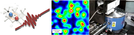
光の量子力学的な性質を利用した量子情報通信の実現に向けて、必要なタイミングに単一の光子を生成する、オンデマンドな単一光子源の開発が強く望まれています。私たちは分子線エピタキシー法を用いてオーダリングしたGaAs表面を原子層窒化することによって、不純物の配列を制御する方法を開発しています。不純物に束縛された励起子からの発光はホスト結晶と不純物の組み合わせで決まる固有の電子状態によって特定の発光波長を示すため、半導体不純物を利用することによって波長のそろった単一光子源の実現が期待できます。またこのような固有の電子状態を有する不純物を利用すれば、スケーラブルな光物性を開拓でき、高効率なもつれ光子対生成も可能になると予想されています。私たちの研究室では、分子線エピタキシー法を用いてオーダリングしたGaAs表面を原子層窒化することによって、不純物の配列を制御する方法を開発しています。具体的には、0.85μm光通信波長帯で動作するGaAs中の窒素不純物に注目し、束縛励起子の電子状態を明らかにするとともに、電子状態の磁場制御について詳細な結果を得ています。これらの成果をもとにして光子相関測定による光子生成の実証を目指しています。さらに、不純物原子配置の制御や多層積層成長技術を駆使して3次元的に制御した空間に不純物を添加することによって、バンド構造を自在に制御する技術を開発しています。
Creation of new semiconductor materials using semiconductor impurities (Kita, Harada)Moving towards the realization of quantum information transmission that uses the quantum mechanical properties of light, the development of an “on demand single-photon” source that generates a single photon in the required time is highly sought after. We are developing a method for controlling the array of impurities by atomic-layer nitridation of GaAs surface atoms that are ordered using Molecular Beam Epitaxy (MBE). The emission from the excitons that were bound to the impurities indicates a specific emission wavelength by an eigen-electronic state determined by the combination of the host crystal and the impurities. So it can be expected that a single photon source having a uniform wavelength can be realized using semiconductor impurities. Furthermore, if we use the impurities that have such eigen electronic states, it is possible to develop scalable optical properties, and it is expected that a highly efficient method of entangled photon pair production would become possible. In our laboratory, we have developed a method for controlling the array of impurities by atomic-layer nitridation of a GaAs surface ordered by the Molecular Beam Epitaxy method. Specifically, we focus on the nitrogen impurities in GaAs operating in the optical communication wavelength band of 0.85μm. In addition to showing the electronic states of the bound excitons, we have obtained detailed results on magnetic field control of electronic states. Based on these results, we aim to demonstrate photon production by photon-correlation measurements. Furthermore, we have developed a technique for controlling the band structure freely by controlling the arrangement of atoms of impurities and by adding impurities in a three dimensionally controlled space using a multilayer stacked growth technique.


同窓会
定期的に開催している同窓会の様子を紹介しております。
ボーリング
スコアを紹介しております。