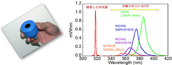
深紫外光源に用いられている水銀ランプは1927年に発明されて以来、今日まで広く使用されており、その応用分野は医療、皮膚治療、殺菌、大面積リソグラフィー、光化学重合、蛍光検査、照明など多岐にわたっています。しかし、水銀ランプは有毒物質である水銀を多量に含んでいるために環境負荷の大きなデバイスであるだけでなく、低いエネルギー利用効率,破裂の危険,短寿命等の課題が山積しています。このような点から水銀を使用しない安全で安心して利用できる代替光源の開発が急務です。最近では水銀ランプの代替光源の1つとして窒化物半導体を使用した紫外発光ダイオードが注目され,盛んに研究されています。発光ダイオードは発光波長をある程度自在に制御可能で、量子井戸構造を導入することによって強い発光を得ることができます。しかし、半導体の基礎吸収端間再結合を利用した発光デバイスでは、注入したキャリアのバンド内でのボルツマン分布により大きなスペクトル拡がりを生じます。このようなスペクトル拡がりは殺菌、架橋、塗料の乾燥などには有効ですが、ナローバンドなスペクトル幅が必要な露光や特定の波長を利用する医療応用(特に皮膚治療では皮膚ガンの発生リスクを抑えるためにスペクトル幅が1nm程度のナローバンド光源を利用した医療が必要とされている)には不向きです。私たちは高効率でナローバンドな深紫外光源を実現するために、蛍光体、固体レーザー、光増幅デバイスなど様々な分野で用いられる希土類イオンに注目しています。希土類イオンの内殻4f軌道遷移発光は電子が充填した外殻によるシールド効果によって外場の影響を受けにくく、ナローバンドな発光を実現します。希土類イオンの中でもf軌道に7つの電子を有するGd(ガドリニウム)イオンは最低励起準位から基底状態への遷移が波長約320 nmの紫外域で発光することが知られており、これをスパッタリング成長によって窒化アルミニウムAlNに添加したものを蛍光体として利用した新しいタイプの紫外光源を開発しています。
Mercury free ultraviolet light sources (Kita)Since its invention in 1927, mercury lamps (used in deep ultraviolet light sources) have been widely used, even today, in diverse fields such as medical treatment, skin treatment, sterilization, large area lithography, photochemical polymerization, fluorescent inspection and lighting. However, since mercury lamps contain a large amount of the toxic substance mercury, not only do these devices cause a huge environmental burden, but also present a bundle of challenges such as low energy utilization efficiency, the risk of explosion and short lifespan. From these points, we see that the need of the hour is the development of a safe alternative light source; and one that can be used peacefully and without the use of mercury. The ultraviolet light-emitting diode that uses a nitride semiconductor has attracted attention as one of the alternate sources of light and has been actively studied in recent years. To some extent, it is possible to freely control the emission wavelength in light-emitting diodes and obtain a strong emission by introducing the quantum well structure. However, in the light emitting devices that make use of the recombination between the fundamental absorption edges of the semiconductor, a large spectral broadening due to the Boltzmann distribution is caused in the band of the injected carriers. Such spectral broadening is effective for sterilization, cross-linking and drying paints. However, they are not suitable for photographic exposure and specific medical treatments (especially in skin treatments that require a narrowband spectral light source with a spectral width of about one nanometer, to reduce the risk of skin cancer) where a narrowband spectrum is required. In order to achieve a narrowband deep ultraviolet light source with high efficiency, we are focused on the rare earth ions that are used in various fields such as phosphors, solid-state lasers, optical amplification devices, etc. The luminescence of the 4f orbital transitions in the inner shells of rare earth ions is less susceptible to external field influence because of the shield effect caused bythe electrons filling the outer shells, and so a narrowband spectral emission can be achieved. Even among the rare earth ions, Gd (Gadolinium) ions that have 7 electrons in the f orbital is known to have transitions from the lowest excitation level to the ground state to emit light in the ultraviolet region with a wavelength of approximately 320 nm. We have developed a new type of ultraviolet light source that uses a phosphor material formed by adding this Gd to Aluminum nitride AIN by means of sputtering growth.
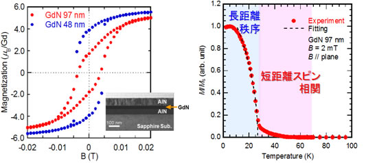
希土類は3価のイオンとなりやすく、その光学的、磁気的特性は内核のf軌道の状態によって決まります。これら希土類元素からなる化合物半導体や合金半導体は光と磁場を介した全く新しい機能の発現が期待されていますが、詳しい物性もいまだ明らかではありません。私たちは白色照明などで最近注目されている窒化物半導体に注目し、希土類窒化物半導体という新しい物質群の創製を行っています。窒化物半導体はⅢ‐Ⅴ族半導体ですので3価の希土類イオンは窒素と結合して安定な窒化物半導体となります。Ⅲ族原子にはAl,In, Gaなどがあり。これらを組み合わせることで合金半導体を作製して、物性を連続的に制御することも可能です。また、ナノ構造を作製することで量子効果を発現させることも期待されています。研究室では超高真空反応性スパッタリングシステムを導入し、極めて高品質な窒化物半導体のヘテロ構造の作製に成功しています。特にGdN/AlNヘテロ構造は近赤外に吸収端を有しながら30K以下では強磁性になる非常にユニークな物質であることが明らかになってきており、これら物質における新規な磁気光学特性の制御の可能性を探索しています。
Development of rare-earth semiconductors(Kita)Rare earth materials easily turn into trivalent ions, and their optical and magnetic properties are determined by the state of the inner f orbital. The compound semiconductors and semiconductor alloys that are composed of these rare earth elements are expected to manifest a completely new function through optic and magnetic fields. However, detailed physical properties are not yet clear. We focused on nitride semiconductors that have been attracting attention recently in areas such as white light illumination, and created a new element group of rare earth nitride semiconductors. Since the rare earth nitride semiconductors belong to the III-V group semiconductors, the trivalent rare earth ion combines with nitrogen to form a stable nitride semiconductor. Al, In and Ga are present in the III group. It is also possible to continuously control physical properties by combining these to form alloys. Furthermore, it is also expected that quantum effects can be manifested by creating nanostructures. In our laboratory, we installed an ultra-high vacuum reactive sputtering system and were successful in creating a hetero structure of an extremely high quality nitride semiconductor. In particular, of late it has been shown that the GdN/AIN heterostructure has an absorption edge in near infrared and also possesses the extremely unique property of becoming ferromagnetic under 30K, and we are exploring the possibilities of controlling the new magneto-optical properties of these substances.
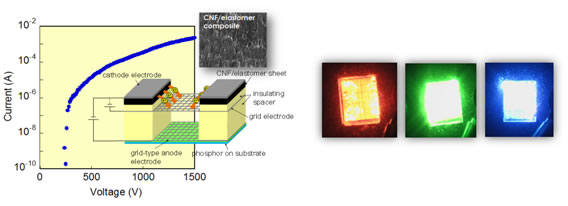
高画質・超低消費電力性を兼ね備えたフラットパネルディスプレイや高輝度で超低消費電力な光源デバイスを実現するために高性能なフィールドエミッターの開発が期待されています。特に競合技術の多いディスプレイデバイス応用とは異なり、フィールドエミッション方式を採用したディスプレイパネル用照明や工業用光源デバイスは低消費電力や水銀フリーなど従来の光源の課題を克服できる特徴を有しており、実用化に近いとデバイスです。しかし従来デバイスを凌駕する安定で精度の高いデバイス動作を実現するにはフィールドエミッションデバイスの精密な構造最適化と課題の精査が不可欠です。私たちは電子源の配置を工夫することでガラス材による吸収を避けた高輝度な光取り出しと、ITOフリーのデバイス構造を同時に実現しています。精密な電界シミュレーションにもとづくデバイス構造の最適化により、現在1平米あたり10万カンデラを超える世界最高クラスの輝度を得ることに成功しています。
Development of high-brightness field emission devices(Kita)Development of high-performance field emitters are expected to realize (a) flat panel displays that have both high-resolution (image quality) and very low power consumption, and (b) light source devices that have high-brightness and very low power consumption. In particular, unlike the application in many display devices of competing technologies, the field emission type light source devices used for illuminating display panels and industrial light source devices have the characteristic of overcoming the problems of conventional light sources like very low power consumption and operating mercury free, and are close to achieving practical usage. However, in order to achieve a stable and highly precise device behavior that surpasses the conventional devices, a careful study of precise structural optimization of field emission devices and its challenges is essential. By devising the arrangement of the electron source, we have simultaneously realized (a) a high-brightness light extraction method that avoids absorption by glass, and (b) an ITO-free device structure. By optimizing the device structure based on precise electric field simulation, we have succeeded in achieving the world's best in-class brightness that is currently more than hundred thousand candela per square meter.
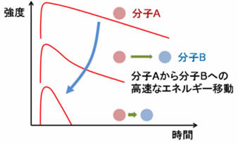
有機色素分子に光を照射すると分子内に励起子状態が形成されますが、この励起子状態はある一定の時間が経過すると元の状態に戻ります。この時間は、主に分子の構造によって決定されますので、目的に応じてこの励起子寿命を制御する必要があります。そのような手法として、エネルギー移動と呼ばれる物理現象に注目しています。これは励起子固有の消滅時間ではなく、強制的に励起状態を異なる分子に乗り移らせる方法です。研究室では、化学的手法を用いて、有機色素とポリマーの多層薄膜を形成し、分子の組み合わせや距離を変えて、励起子が消滅する時間を制御しています。このような手法を用いて、特に、長短パルスを極短時間内に繰り返し照射しても使用可能な超高速光デバイスの実現を目指しています。
Development of organic dye thin film materials using energy transfer(Kojima)If organic dye molecules are irradiated with light, exciton states are formed inside the molecules. These exciton states will return to their original states after a certain period of time elapses. This time period is primarily determined by the molecular structure, and so it is necessary to control exciton lifetimes depending on our objective. As one such an approach, we are focusing on a physical phenomenon called energy transfer. This is not an exciton-specific annihilation time, and is a method for the forcible transfer of an exciton state to a different molecule. In our laboratory, we use chemical methods to form a multilayer-thin film of polymers and organic dyes, and we control the annihilation time of excitons by changing molecular combination and distance. With these approaches, we are working particularly towards realizing ultra-high-speed optical devices that can be used even when irradiated by repeating long and short pulses in an extremely short period of time.
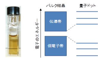
コロイド量子ドットは、化学的に合成されたナノメートルサイズの半導体微結晶であり、溶液プロセスが適用可能であるという特徴をもっています。そのため、コロイド量子ドットを利用した太陽電池や発光・受光素子のフレキシブル基板上への大量生産が、スピン塗布やスプレー塗布といった既存のプリント・塗布技術によって実現できると期待されています。また量子ドットでは電子・正孔の運動の自由度が制限されるため、電子状態が量子ドットのサイズによって変化します。私たちの研究室では、電子と正孔の両方が量子閉じ込め効果を強く受けるPbSコロイド量子ドットに注目し、ポリマー薄膜に埋め込まれたPbSコロイド量子ドットにおける光物性の解明と新規光機能デバイスの実現を目指しています。
Development of optical functional materials using colloidal quantum dots(Harada)Colloidal quantum dots are chemically synthesized nanometer-sized semiconductor nanocrystals that have a characteristic feature such that solution processes can be applied to them. Therefore, it is expected that mass production of solar cells and flexible substrates of light emitting and receiving elements that use colloidal quantum dots can be realized using existing print/coating techniques like spin coating and spray coating. Furthermore, since the degree of freedom of motion of electrons and holes is restricted in quantum dots, their electronic states will change depending on the size of the quantum dot. In our laboratory, we focus on the PbS colloidal quantum dots where both electrons and holes are impacted by a strong quantum confinement effect, and we work towards elucidating the optical properties of PbS colloidal quantum dots embedded in polymer thin films, and realizing new optical functional devices.


同窓会
定期的に開催している同窓会の様子を紹介しております。
ボーリング
スコアを紹介しております。