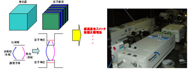
半導体の構造をナノメートルスケール(1ナノ=10-9)で制御すると、量子閉じ込め効果により、電子状態が変化します。近年、この量子効果を利用した様々な光デバイスが作製されています。例えば、光情報通信において、より高速で信号処理を行うための超高速光スイッチや新世代の太陽電池などが挙げられます。そのようなより高性能な光デバイスを実現するためには、量子構造における光の吸収や光により生成された電子などの消滅過程を明らかにすることが重要となります。これらの過程を明らかにするために、超高速分光手法が必要となってきます。極短時間内で起こる物理現象を観測する場合、従来の電子機器では観測できなくなります。これは、機器に使用する素子の電子の移動度などで、時間分解能が決定されるためです。近年、レーザー技術の発達により、100フェムト秒(1フェムト=10-15: 光がわずか30mを進む時間)程度のパルス幅をもつ光パルスを使用することができるようになりました。これにより、さまざまな超高速分光手法が開発されました。その結果、テラヘルツ電磁波放射や種々のコヒーレント現象など、新しい光現象が次々と報告されるようになりました。我々の研究室では、半導体薄膜、多重量子井戸構造および量子ドットなどにおける励起子(電子と正孔のペア)のフェムト秒の時間スケールでの光応答特性の解明と制御を中心に、徳島大学、独立行政法人情報通信研究機構およびイギリスのシェフィールド大学などと共同で研究を展開しています。
NanophotonicsWhen the semiconductor structure is controlled at the nanometer scale (1 nanometer = 10-9 ), electronic states will change due to the quantum confinement effect. Various optical devices that use quantum effects have been produced in recent years. The ultrafast optical switches for faster signal processing in the optical information communication systems and new generation solar cells can be cited as examples of these. To realize such high-performance optical devices, it is important to elucidate the annihilation process of electrons generated by light and absorption of light in the quantum structure. Ultrafast spectroscopy techniques are necessary to elucidate these processes. The physical phenomena that occur within a very short time cannot be observed using conventional electronic equipment. This is because the time resolution is decided by the mobility of electrons in components that are used in the equipment. In recent years, owing to the developments in laser technology, it is possible to use light pulses with a pulse width of about 100 femtoseconds (1 femto = 10-15 , the time that light takes to travel a distance of just 30 x 10-8m ). This has resulted in the development of various ultra-fast spectroscopic techniques. As a result, many new optical phenomena such as terahertz electromagnetic radiation and a variety of coherent phenomena have been reported, one after the other. In our laboratory, we focus on elucidating and controlling the optical response characteristics on the time scale of femtoseconds of excitons (electrons and hole pairs) that occur in semiconductor thin films, multi-quantum well structures and quantum dots. We are carrying out research in collaboration with Tokushima University, the National Institute of Information and Communications Technology (NICT), and The University of Sheffield in United Kingdom.
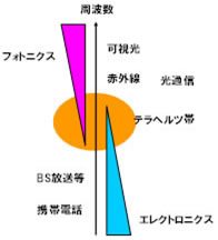
周波数がテラヘルツ(1テラ=1012)の電磁波は、テラヘルツ電磁波と呼ばれ、エレクトロニクスとフォトニクスを繋ぐ周波数帯の電磁波として注目されており、現在、様々な分野への応用が期待されている周波数の電磁波です。この電磁波は、半導体に超短パルスレーザーを照射することで発生させることができます。また、最近では、連続波レーザーを使用して、テラヘルツ電磁波を連続的に発生させる手法も提案されています。研究室では、励起子量子ビートと呼ばれる半導体内部におけるコヒーレント振動現象に注目し、この量子ビートから発生するテラヘルツ電磁波放射に関する研究を行っています。量子ビートを利用することで、周波数を自在に制御できるテラヘルツ電磁波発生デバイスへと展開することができます。量子ビートは励起子の位相緩和の克服が課題ですので、室温でテラヘルツ電磁波を発生させるための基礎特性の解明を行っています。また、テラヘルツ電磁波を効率よく検出するための検討も行っています。
Terahertz electromagnetic wave radiation from semiconductorElectromagnetic waves in the frequency of terahertz (1 tera =1012) are referred to as terahertz electromagnetic waves. These THz waves have attracted attention as electromagnetic waves with the right frequency band to connect electronics and photonics. These electromagnetic waves, with characteristic frequencies, are expected to be applied to various fields in the future. These waves can be generated by irradiating an ultra-short pulse laser on a semiconductor. Furthermore, a method of generation of terahertz waves continuously using a continuous wave laser has also been proposed recently. In this laboratory, we focus on the phenomenon of coherent oscillations inside the semiconductor called excitonic quantum beats and are researching the THz electromagnetic radiation generated from these quantum beats. Using quantum beats, we can move towards developing a terahertz electromagnetic wave generating device that can independently control the frequency. Since overcoming the phase relaxation of quantum beats is a major challenge, we are working on elucidating the basic characteristics required for generating THz electromagnetic waves at room temperature. In addition, we are also carrying out studies detecting THz electromagnetic waves more efficiently.
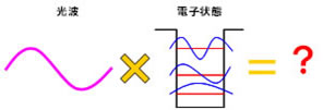
半導体の構造をナノメートルオーダーで制御することで、励起子状態を制御できます。この励起子を使って、光→励起子(電子系)→光といった変換過程を制御し、それにより非線形光学応答の制御を目指します。特に、超高速光スイッチや量子情報デバイスなどでは、光で励起子状態を制御するコヒーレント制御と呼ばれる技術の実現が必要です。研究室では、様々な半導体を試料に用い、四光波混合法やポンプ・プローブ法により励起子応答特性測定を評価し、新しい半導体構造の設計を行っています。
Coherent control in semiconductor thin films and multi-well structuresExcitonic states can be controlled by directing the semiconductor structure on the order of nanometers. Using these excitons, we control the conversion process of light→ exciton (electron system) → light and aiming to control the non-linear optical response. In particular, in ultrafast optical switches and quantum information devices, it is necessary to realize a technique called coherent control for directing the excitonic states in light. In our laboratory, we are working on designing a new semiconductor structure using a variety of semiconductor samples and evaluating their measured excitonic response characteristics with a four-wave mixing method as well as pump-probe methods.
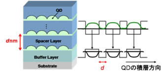
半導体基板上に多層積層した量子ドットでは、試料成長方向の量子ドット間距離をさまざまに変えることで光物性を制御できることを明らかにしています。ここで重要なのは、デバイスへ応用する際に必要とされる光物性を明らかにすることです。研究室では、様々な条件で生成した光生成キャリアの緩和過程や発光特性を解明することで、物性制御とデバイス応用を有機的に関連付けることを目指しています。
Controlling the optical properties in a multilayered quantum dotIn quantum dots that have been stacked as multiple layers onto semiconductor substrates, it is possible to control the optical properties by varying the distances between the quantum dots that are in the direction of sample growth. Here, it is important to reveal the optical properties that are necessary for device application. In our laboratory, we are working towards elucidating the emission characteristics and the optical carrier relaxation process of the carriers generated under various conditions and aim to establish a relationship between the control of physical properties and application to devices.
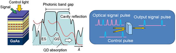
半導体多層膜で高い反射率を有する鏡を作製し、それを使って共振器を作製します。この共振器の中に量子ドットなどを挿入し、光応答時間を制御します。共振器の共振波長を設計し、量子ドットの光応答波長との関係をいろいろ変えて、超高速光スイッチへの応用を目指しています。
Development of an ultrafast optical switch that uses a resonator structureWe create a mirror with high reflectance, using a semiconductor multilayer film and then constructing a resonator with it. Then, we insert the quantum dots within this resonator and control the optical response time. Next, we design the resonance wavelength of the resonator, and by varying the relation between the optical response wavelengths of the quantum dots, we aim to apply this to ultrafast optical switches.


同窓会
定期的に開催している同窓会の様子を紹介しております。
ボーリング
スコアを紹介しております。