量子物理に基づくモデリングと実装
Quantum Physics, Modeling, and Device Implementation
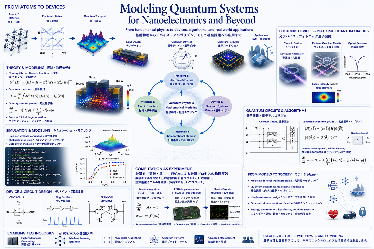
半導体デバイスの微細化と量子技術の発展に伴い、電子や量子状態の振る舞いを物理学に基づいて理解し、それを材料・デバイス・回路・量子システムの設計へと結びつけることが、従来にも増して重要になっています。当研究室では、量子力学、電子輸送理論、数理モデリング及び数値計算を基盤として、ナノ・半導体デバイス、新材料デバイス、半導体量子ビット、開放量子系、量子アルゴリズム及び量子ハードウェアに関する研究を進めています。研究においては、計算結果を得ることだけを目的とするのではなく、対象となる物理系の本質をどのように数理モデルとして切り取り、そのモデルをどのような計算方法及びハードウェアによって実現するか、という一連の過程を重視しています。
As semiconductor devices continue to shrink and quantum technologies advance, it is becoming increasingly important to understand the behavior of electrons and quantum states on the basis of physics and to connect that understanding to the design of materials, devices, circuits, and quantum systems. Our laboratory conducts research on nanoelectronic and semiconductor devices, emerging-material devices, semiconductor qubits, open quantum systems, quantum algorithms, and quantum hardware, using quantum mechanics, electron transport theory, mathematical modeling, and numerical computation as its foundations. Our aim is not merely to obtain numerical results, but to clarify how the essential physics of a target system should be represented as a mathematical model and how that model can be realized through computation and hardware.
-- ナノ・半導体デバイスの量子輸送シミュレーション
Quantum-Transport Simulation of Nanoelectronic and Semiconductor Devices
半導体デバイスの寸法がナノメートル領域に到達すると、電子の波動性、トンネル効果、量子閉じ込め、電子・フォノン散乱などがデバイス特性を直接的に決めるようになります。このため、その動作原理や性能限界を明らかにするには、量子輸送理論に立脚したデバイスシミュレーションが不可欠です。当研究室では、非平衡グリーン関数法、モンテカルロ法、量子補正法、時間依存量子輸送法などを用いて、MOSFET、TFET、ナノワイヤデバイス、低次元材料デバイスなどの電子状態及び電子輸送を解析しています。また、デバイス単体の特性だけではなく、回路動作との連携を見据えたモデリング及びシミュレーションにも取り組んでいます。
When semiconductor-device dimensions enter the nanometer regime, electron wave behavior, tunneling, quantum confinement, and electron-phonon scattering directly determine device characteristics. Quantum-transport-based device simulation is therefore indispensable for clarifying operating principles and ultimate performance limits. We use the nonequilibrium Green's function method, Monte Carlo methods, quantum-correction approaches, and time-dependent quantum-transport methods to study the electronic states and transport properties of MOSFETs, TFETs, nanowire devices, and low-dimensional-material devices. We also develop modeling and simulation frameworks that connect individual device characteristics with circuit-level operation.
-- 新材料・原子論的電子状態及びデバイス設計
Emerging Materials, Atomistic Electronic Structure, and Device Design
ナノメートルサイズは原子数個から数十個程度の大きさに相当するため、新材料及びナノデバイスの設計においては、個々の原子配置や化学結合を反映した原子論的な取り扱いが重要になります。当研究室では、強束縛近似法(タイトバインディング法)及び第一原理計算法を用いて、原子構造、バンド構造、局所状態密度、電子輸送特性の関係を解析しています。対象とする材料は、シリコン及びSiCに加え、グラフェン、グラフェンナノリボン、TMDC、フォスフォレンなどの低次元材料に及びます。これらの解析を通じて、新材料を用いた電子デバイス及び光デバイスの設計指針を明らかにすることを目指しています。
Because nanometer-scale structures may contain only a few to a few tens of atoms across their characteristic dimensions, atomistic descriptions that reflect atomic configurations and chemical bonding are essential for the design of emerging materials and nanodevices. We use tight-binding methods and first-principles calculations to analyze the relationships among atomic structure, band structure, local density of states, and electron-transport properties. Our target materials include silicon and SiC, as well as low-dimensional materials such as graphene, graphene nanoribbons, transition-metal dichalcogenides, and phosphorene. Through these studies, we seek to establish design principles for electronic and photonic devices based on emerging materials.
-- 半導体量子デバイスと量子ビット実装
Semiconductor Quantum Devices and Qubit Implementation
量子コンピューティングにおいては、量子ビットを構成する物理系をどのように作り、量子状態をどのように生成・操作・読み出すかが本質的な課題になります。当研究室では、半導体量子ドット、スピン量子ビット、グラフェンナノリボン量子ドット及びフライング量子ビットなどを対象として、単一電子輸送、量子状態制御、デコヒーレンス及びデバイスばらつきに関する研究を進めています。量子ビットを抽象的な情報単位としてのみ扱うのではなく、その物理的実体となる材料、電子状態及びデバイス構造との関係を明らかにすることを重視しています。
A central challenge in quantum computing is how to create the physical systems that form qubits and how to generate, manipulate, and read out their quantum states. We study semiconductor quantum dots, spin qubits, graphene-nanoribbon quantum dots, and flying qubits, with particular attention to single-electron transport, quantum-state control, decoherence, and device variability. Rather than treating a qubit only as an abstract unit of information, we emphasize its connection to the material, electronic structure, and device architecture that provide its physical realization.
-- 開放量子系と量子ダイナミクスの数理モデリング
Mathematical Modeling of Open Quantum Systems and Quantum Dynamics
現実の量子系は周囲の環境から完全に切り離されているわけではなく、散逸、測定、雑音及びデコヒーレンスの影響を受けます。当研究室では、開放量子系の時間発展、量子チャネル、測定・リセットを含む量子回路表現、量子輸送と量子情報の接続などについて研究しています。特に、物理系の時間発展をどのような数理モデルとして定式化し、それを古典計算及び量子回路上でどのように表現するかを検討することで、量子デバイスと量子アルゴリズムを物理の立場から結びつけることを目指しています。
Real quantum systems are never completely isolated from their surroundings and are affected by dissipation, measurement, noise, and decoherence. We study the time evolution of open quantum systems, quantum channels, quantum-circuit representations that include measurement and reset operations, and connections between quantum transport and quantum information. In particular, we investigate how the dynamics of physical systems should be formulated as mathematical models and how those models can be represented in classical computation and quantum circuits, thereby connecting quantum devices and quantum algorithms from a physics-based viewpoint.
-- 光デバイスとフォトニック量子回路
Photonic Devices and Photonic Quantum Circuits
光と物質の相互作用を用いるデバイスは、通信、センシング、情報処理及び量子技術において重要な役割を持っています。当研究室では、導波路、共振器、受発光デバイスなどの光デバイスに加え、光子を用いた量子状態操作及びフォトニック量子回路のモデリングに関する研究を進めています。電磁場分布、共振特性、光学応答及び量子状態の伝搬を数理的・計算科学的に解析し、材料・構造・デバイス・量子回路を一貫して理解することを目指しています。
Devices based on light-matter interaction play important roles in communications, sensing, information processing, and quantum technologies. Our research covers photonic devices such as waveguides, resonators, photodetectors, and light-emitting devices, as well as the modeling of photon-based quantum-state manipulation and photonic quantum circuits. By analyzing electromagnetic-field distributions, resonance characteristics, optical responses, and the propagation of quantum states, we aim to develop a unified understanding that connects materials, structures, devices, and quantum circuits.
-- 物理シミュレーションと機械学習の融合
Integration of Physics Simulation and Machine Learning
ナノデバイス及び量子系の高精度シミュレーションには、大規模な数値計算が必要になる場合があります。当研究室では、量子輸送計算やデバイスシミュレーションの高速化・高精度化を目的として、機械学習及びデータ駆動型手法の利用を進めています。ただし、機械学習によって物理計算を単純に置き換えることを目的とするのではなく、支配方程式、境界条件、対称性、保存則などの物理的・数理的構造を考慮しながら、数値計算と機械学習をどのように組み合わせるべきかを重視しています。
High-accuracy simulations of nanodevices and quantum systems often require large-scale numerical computation. We therefore investigate machine-learning and data-driven approaches for accelerating and improving quantum-transport and device simulations. Our goal is not simply to replace physics-based computation with machine learning, but to determine how numerical methods and learning-based methods should be combined while respecting governing equations, boundary conditions, symmetries, conservation laws, and other physical and mathematical structures.
-- 計算を「実験する」― FPGAによる計算プロセスの物理実装
Computation as Experiment: Physical Realization of Computational Processes Using FPGA
通常の数値計算では、方程式やアルゴリズムはソフトウェア上で実行され、その計算過程そのものを物理現象として意識することは多くありません。一方、FPGA上に計算プロセスを実装すると、数値モデルは電圧、電流、遅延、並列動作及びエネルギー消費を伴う現実の物理過程として実現されます。当研究室では、微分方程式や反復計算などをFPGA上の回路として構成し、計算過程そのものを観測・評価することで、「計算を実験する」という新しい考え方を探究しています。これは単なる高速計算ではなく、計算モデル、ハードウェア及び物理現象の関係を改めて問い直す試みです。
In conventional numerical computation, equations and algorithms are executed in software, and the computational process itself is rarely regarded as a physical phenomenon. When a computational process is implemented on an FPGA, however, the numerical model is realized as an actual physical process involving voltage, current, delay, parallel operation, and energy consumption. We implement differential equations, iterative processes, and related models as FPGA circuits and observe and evaluate the computation itself. This “computation as experiment” approach is not merely a method for high-speed computation; it is an attempt to reconsider the relationship among computational models, hardware, and physical phenomena.
-- 量子数理モデルと量子ハードウェアの連携―社会課題への展開
Linking Quantum Mathematical Models with Quantum Hardware for Societal Applications
量子コンピューティングを実社会の問題に応用するためには、対象となる問題をどのような量子数理モデルとして表現するか、また、そのモデルを現実の量子ハードウェア上でどのように実行・検証するかを一体として考える必要があります。当研究室では、最適化、材料・エネルギー、センシング、通信などの社会課題を念頭に、量子アルゴリズムの設計、量子回路への変換、ノイズ及びハードウェア制約の取り込み、古典計算との連携に関する研究を進めています。数理モデル、アルゴリズム及び物理実装を切り離すのではなく、それらを往復しながらモデルを改善していくことを重視しています。
Applying quantum computing to real-world problems requires the problem to be formulated as an appropriate quantum mathematical model and that model to be executed and verified on actual quantum hardware. With societal challenges in areas such as optimization, materials and energy, sensing, and communications in mind, we study quantum-algorithm design, mapping to quantum circuits, incorporation of noise and hardware constraints, and integration with classical computation. Rather than separating mathematical models, algorithms, and physical implementation, we emphasize an iterative process in which each is refined through feedback from the others.